As always you find the design files on my GitHub.
Designing a sensor that meets the specific requirements of a particular application involves overcoming several
hardware challenges. From creating a Printed Circuit Board (PCB) using Computer-Aided Engineering (CAE) software to
carefully selecting the right components, every step in the design process is crucial. Additionally, designing for
manufacturing adds another layer of complexity. In this blog post, we will delve into the intricacies of tackling these
hardware challenges, exploring the essential considerations and techniques involved in crafting a successful sensor
design.
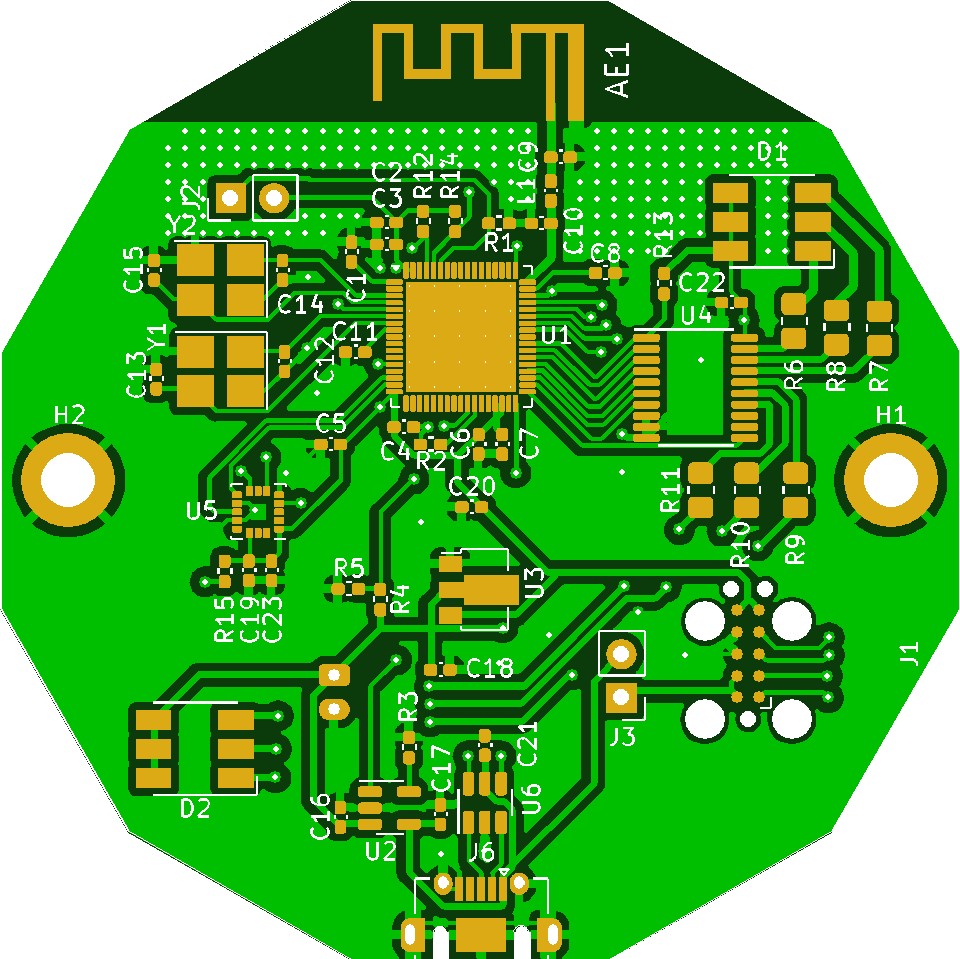
The design of the sensor encompasses several key components, each playing a crucial role in its functionality and
performance. These components include the microcontroller, power management system, visual feedback module, proximity
sensing unit, and RF frontend. Ensuring the seamless integration of these components within a suitable enclosure presents
a significant challenge. Considering that mechanical lead times often pose a bottleneck in the design process, a signal
light was chosen as the ideal enclosure. In the subsequent paragraphs, we will delve into each of these sections
individually, exploring their intricate details and considerations.
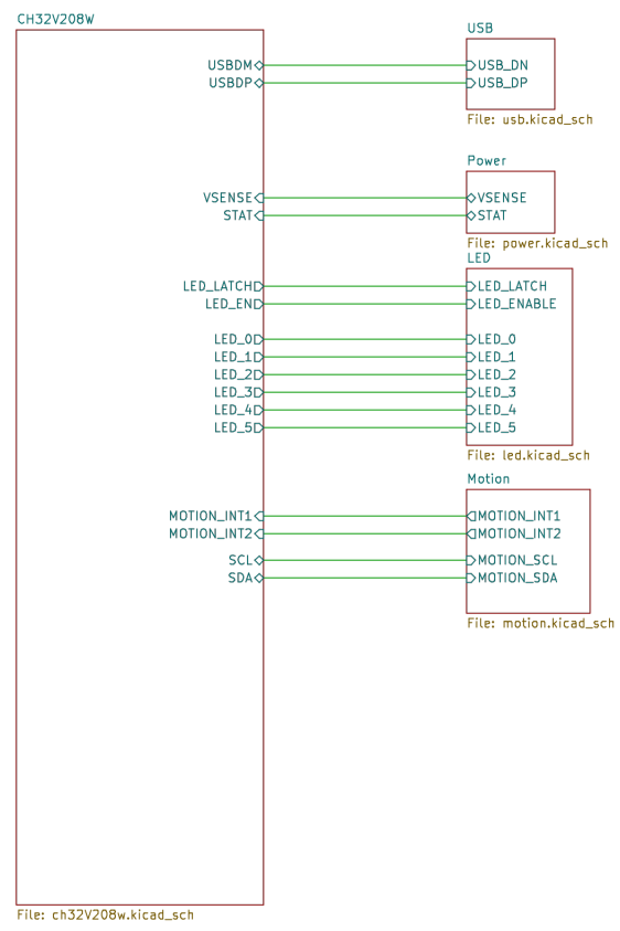
The Microcontroller
As a participant in the contest, I have made a deliberate choice to utilize the CH32V208W platform for my project. This
platform features a 32-bit RISCV controller renowned for its affordability and versatility, offering a rich selection of
peripheral interfaces to cater to a wide range of requirements. Specifically tailored for this contest, the essential
peripherals I will be utilizing include an on-chip RF peripheral with a proprietary library, enabling seamless integration
of the Bluetooth Low Energy interface. Additionally, an I2C interface will be employed to connect an accelerometer, an
ADC will facilitate power sensing, a USB connection will allow for factory flash and firmware upgrades, and additional
pins will be allocated for driving high-power LEDs, providing comprehensive visual feedback. By leveraging the
capabilities of the CH32V208W platform and carefully selecting the necessary peripherals, I aim to create an
efficient and effective solution for this contest.
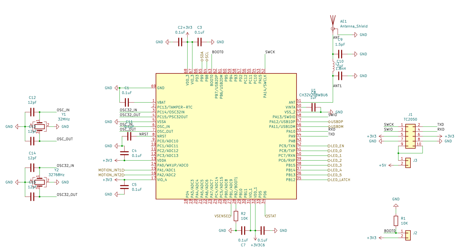
The presented diagram illustrates the essential circuitry encompassing the microcontroller. In the case of this
particular chip, the requirements are relatively straightforward, consisting of a few stabilizing capacitors and
external oscillators to ensure precise timing for both the USB and RF front end. While the chip does feature internal
oscillators that could potentially enable autonomous operation, it remains imperative to incorporate at least one
high-speed external oscillator to guarantee accurate timing for USB and RF functionalities. Although the inclusion of
a 32768Hz oscillator is optional, I opted to adhere to the development kit specifications in order to mitigate any
potential design risks. Once the debug interface is enabled via the WCH ISP tool, the debug connector no longer
necessitates a reset line. The bootloader is activated by bridging BOOT0 to VCC or closing J2. It is worth noting
that the chip is conveniently available in a QFN-68 package from LCSC. However, due to the challenging nature of
hand soldering, I have decided to enlist the services of JLC-PCB to handle the entire assembly process, ensuring
optimal results and reliability.
One issue that was not documented was the inclusion of the VINT capacitor for the internal regulator. The development
kit at a 1uF capacitor. Since I am cheap and want to save on feeder setup fees, I added a 10uF capacitor instead to
share volume across other parts of the design. Fingers crossed, this will work.
The RF Frontend for Bluetooth Low Energy
The above schematic shows antenna design and guestimated antenna matching. Nanjing Qinheng Microelectronics (WCH) provides guidance in Chinese on how to lay out an inverted F-antenna. I found a well-maintained library for several
WCH footprints, including the antennas from Sad Electronics. I forked it to add schematic symbols for the CH32V208 and
adapt the antenna footprints for existing Kicad schematic antenna symbols. Expect a merge request, once the design works. Infineon has a good application note on the design theory behind it. Putting the footprint in place is less than half
the battle for RF design. The bigger challenge is calibrating the layout to the environment, as minuscule changes in
the PCB dielectric or ground plane will throw the reference design out of calibration. Texas Instruments has a good application note for this. Because the
ground plane next to the IFA section is critical I used this plugin to generate strips of vias in the plane.
The USB Interface
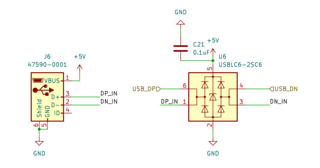
The USB interface is fairly straightforward. Since I do not require high-speed USB, I did not route the USB interface
explicitly as differential pair and eyeballed it instead. Make sure you have ample ground-planes and around the trace
pairs. This should be ok. To protect against accidental electronic discharge, I put a TVS array right behind the
USB connector.
Power
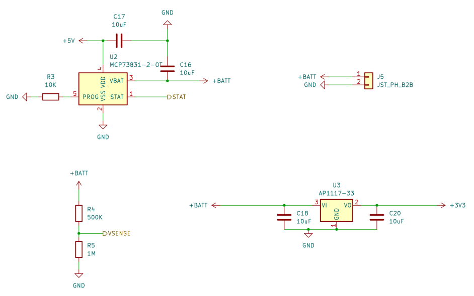
The power design for the sensor follows a relatively straightforward approach. To enable independent operation, a
lithium polymer battery has been selected as the power source. Whenever the sensor is externally connected via USB,
the battery is charged, and it directly supplies power to the high-power LEDs. Furthermore, the battery voltage is
stepped down to 3.3V, which powers the microcontroller and other peripherals. It is important to note that this voltage
dropout may not be ideal, considering that lithium batteries can discharge as low as 3.0V. However, this design decision
was made to maintain consistency with the development kit and minimize deviations. In a future sensor revision, a
significant reworking of this aspect is expected. To minimize battery discharge when the microcontroller is in low-power
standby mode, an LDO (Low Dropout) regulator with a minimal quiescent current was carefully chosen, ensuring efficient
power management.
Visual Feedback
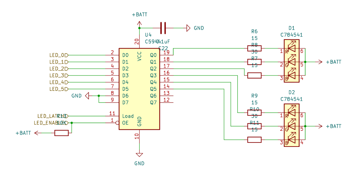
For visual feedback to the user, a pair of high-power LED arrays was chosen. Since the microcontroller does not have the
drive strength to drive the LEDs directly, the output is buffered using a 74573 logic buffer. This is a classic design
from lost Intel 8051 days when microcontroller pins were in short supply, the logic latch can be enabled and disabled,
freeing up the pins for other purposes. The 74HC logic levels permit a 3.3V logic input on one side and can drive higher
voltages on the other side, making this a low-cost logic-level translator at the same time.
Motion Sensing
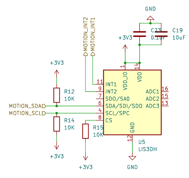
Motion sensing is performed by an accelerometer from ST. The choice
was essential fell on what is in stock and low-cost
at LCSC. So I found this ST accelerometer that can interrupt the microcontroller when a certain acceleration (i.e. shock,
smack…) is reached and provide haptic feedback to the user that a leg of their exercise routine has been completed.
Enclosure
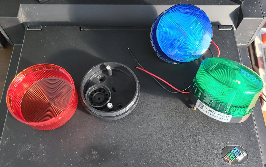
Since I did not have the time to design a fully-fledged enclosure the PCB was designed to fit a signal light. The N-3071 line of signal lights
provides a low-cost platform for the enclosure, even considering that you discard the
original circuit. I tried to source lights that have a clear acrylic cover but could not source them in time.
Conclusion
This concludes the system overview of the electrical design of the sensor. I initially planned to include proximity
sensing via an infrared distance sensor as well as audible feedback from an I2S amplifier and a speaker too, but I
did not have enough space to route that out inside the chosen enclosure. In the next revision, these features may be
added. The upcoming article will outline the software stack using RT-Thread.
Published: 2023-06-06
Updated : 2025-10-04
Not a spam bot? Want to leave comments or provide editorial guidance? Please click any
of the social links below and make an effort to connect. I promise I read all messages and
will respond at my choosing.