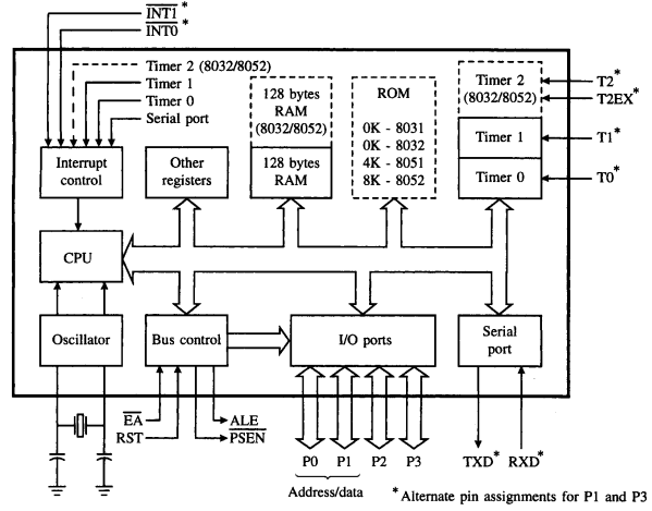
This article is written in support of the GPIO tool I wrote for the MCS-51 series. Most of the MCS-51
derivatives have a similar GPIO architecture, so this article should be applicable to most of them. I plan to update
this with other topologies as more modern microcontrollers get covered on this blog.
Quasi-Bidirectional GPIOs
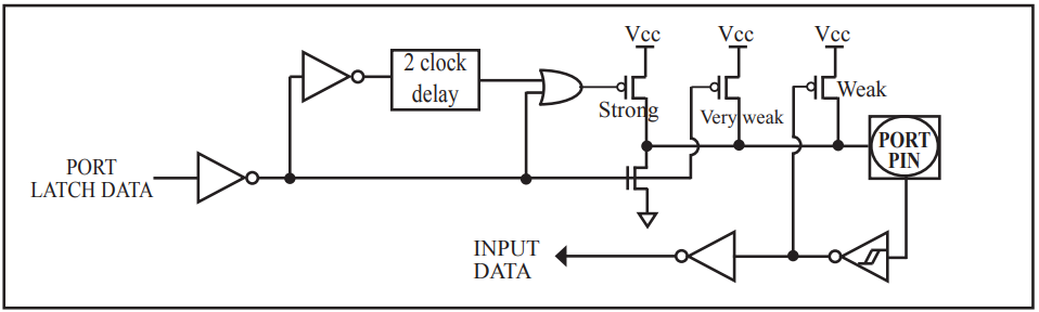
The quasi-bidirectional port is associated with the classic 8051 microcontroller. It was engineered as a silicon-efficient
solution to create a port that could function as both an input and an output without requiring a separate data direction
register for each pin. The design dates back to the 70s, when the 8051’s predecessor (the 8048) was developed;
minimizing transistor count and silicon area was a primary goal. Registers are one of the most transistor-intensive components
of a semiconductor, even recent attempts to democratise waver-scale design have highlighted this.
- “Very Weak” Pull-up: This transistor is turned on whenever the port’s output latch is set to ‘1’.
It sources a very small current (tens of microamperes) sufficient to pull the pin high if it is left floating, but is
easily overpowered by an external device. This ensures an unconnected pin does not float.
- “Weak” Pull-up: This transistor is active only when the port latch contains a ‘1’ and the pin’s voltage is
already at a logic high level. It provides the primary sustaining source current for an outputting ‘1’ state. If an
external device pulls the pin low, this weak pull-up turns off, leaving only the very weak pull-up active. The external
device must sink enough current to overcome this pull-up to register as a logic low.
- “Strong” Pull-up: This transistor provides a brief, high-current pulse to accelerate the pin’s low-to-high transition.
It is activated for one or two clock cycles immediately after the port latch is changed from a ‘0’ to a ‘1’, charging
any line capacitance. This helps to speed up rising edges.
To use the pin as an input, write a ‘1’ to the port latch bit. The pin is then held high by default but can be easily
pulled low by an external circuit. You can ead the pin’s actual state via its input buffer.
To use the pin as an output, writing a ‘0’ to the latch activates the strong pull-down transistor, creating a definitive
logic low output. Writing a ‘1’ activates the weak pull-up network to create a logic high.
This makes drive strength is therefore highly asymmetrical: strong when pulling low (sinking several milliamps), but weak
when pulling high (sourcing only tens of microamperes).
On the classic 8051, Ports 1, 2, and 3 are quasi-bidirectional. Port 0, however, is an open-drain port and requires
external pull-up resistors to produce a logic high level. This limitation is however not the case for most modern
MCS-51 derivatives. Note the AT89C5x series and STC89C5x follow this traditional pattern and cannot be reconfigured
to anything else, despite claims in the STC datasheet.
Push-Pull GPIOs
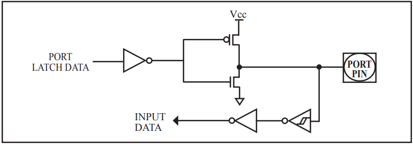
This is common output type in modern microcontrollers. It has a strong symmetric drive capability.
A push-pull output stage is implemented using a pair of complementary transistors . This structure is often referred to
as a “totem-pole” output. When the pin is set to a logic HIGH, the high MOSFET connects the pin to VDD, actively
sourcing current. Conversely, for a logic LOW, the MOSFET connects the pin to GND, actively sinking current. In
either state, one transistor is ON while the other is OFF.
The primary advantage of the push-pull architecture is its ability to actively drive the output in both directions.
This active sourcing and sinking of current results in a low-impedance output state, which enables fast signal rise
and fall times by quickly charging and discharging the parasitic capacitance of the connected load. This makes it the
preferred configuration for high-speed, point-to-point communication protocols like SPI and UART, as well as for directly
driving components that require significant current, such as LEDs.
However, this is unsuitable for shared bus systems (use quasi-bidirectional or open-drain instead). If two push-pull outputs are
connected to the same wire and one attempts to drive the line HIGH while the other
drives it LOW, a direct, low-impedance path is created between VDD and GND through the two active transistors.
It results in a short circuit that can cause excessive current draw, potentially leading to permanent damage.
Open Drain or Open Collector GPIOs
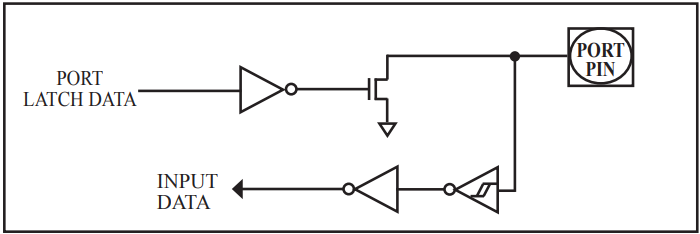
Open-drain provides a solution for applications where multiple devices must share a single communication line.
The drain of the pull-down transistor is left unconnected to any internal pull-up source. The output
consists of a single MOSFET that connects the port to ground. Unlike push-pull, there is no complementary MOSFET to pull
the port to VDD. When the output is LOW, the MOSFET is activated, pulling the port to ground.
When the output is HIGH, the MOSFET is deactivated, leaving the pin in a high-impedance state, effectively floating.
Because the device can only actively pull the line low, an external pull-up resistor connected between the pin and VDD is required to establish the logic HIGH state. When all devices on the line are in their high-impedance
state, the resistor pulls the pin to VDD. This enables a “wired-AND” functionality:
- The bus line will be
HIGH only if all connected devices are in their high-impedance state. - If any single device activates its MOSFET to pull the line low, the entire bus line will go
LOW.
This is the foundational principle that allows for multi-master communication, arbitration, and clock stretching in
protocols like I2C or Dallas one-wire.
The selection of the external pull-up resistor value is a critical design decision involving a trade-off between speed
and power consumption. A low-value resistor allows for faster rise times by more quickly charging the line capacitance,
enabling higher bus speeds. However, it also results in higher static power dissipation when the line is pulled low, as
more current flows from VDD through the resistor and the active MOSFET to GND. A high value minimizes static
power consumption but results in a slower rise time, which can limit the maximum operating frequency of the bus. Check
with your bus specification for recommended values and assumed bus capacitance. Phillips, ehm now NXP,
has a good Application Note on this topic.
The input-only, or high-impedance, mode provides the purest form of digital sensing. In this configuration,
both of the output transistors are turned off, making the pin a very high impedance to the external circuit.
The input path consists of protection diodes and a Schmitt trigger buffer. The Schmitt trigger provides input hysteresis,
meaning it has different voltage thresholds for detecting a rising edge (VIH) versus a falling edge (VIL).
This feature improves noise immunity.
This mode is optimized for low power consumption. By disabling all output drivers and internal pull-up resistors,
it eliminates current paths that can exist in other modes. For instance, a quasi-bidirectional port configured as an
input will continuously draw a small current from its internal pull-up if the external signal is held LOW, whereas a
true high-impedance input will not.
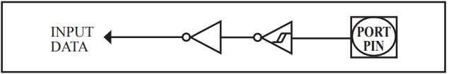
A feature of most GPIO topologies is that the input buffer remains connected to the physical pin even when the pin is
configured as an output. This allows the microcontroller to read the actual voltage level of the pin at any time.
The ability to read the pin’s physical state differs from reading the internal output latch. Reading the latch simply
returns the last logic value written to the port by the software. Reading the pin, however, returns the actual logic
level present on the physical pin, which can be influenced by the external load.
For example, if a push-pull output is set to HIGH but is connected to a load that sinks more current than the pin
can source, the pin’s voltage may drop below the microcontroller’s input high threshold (VIH). In this scenario,
reading the output latch would return a ‘1’, while reading the pin’s input data register would return a ‘0’.
Summary
This article provided an overview of the various GPIO configurations commonly found in MCS-51 derivatives. Check out
the GPIO tool that provides basic code generation for various MCS-51 derivatives and their GPIO configurations.
In future there is going to be more on what topologies are useful for driving various loads and interfacing with different peripherals.
Good references for further reading:
Published: 2025-10-22
Updated : 2025-10-25
Not a spam bot? Want to leave comments or provide editorial guidance? Please click any
of the social links below and make an effort to connect. I promise I read all messages and
will respond at my choosing.