Going back to my vintage, Philips Semiconductors (now NXP) was a major player in the embedded systems world. They created
a number of popular devices, including microcontrollers, memory chips, and various peripherals. One of their most significant contributions
was the development of the I2C (Inter-Integrated Circuit) bus, a widely used communication protocol in embedded systems.
Unlike Dallas 1-Wire (which was developed later), I2C uses two lines: a serial data line (SDA)
and a serial clock line (SCL). This allows multiple devices to be connected on the same bus, each with a unique
address. There are several generations of the I2C protocol, with speeds ranging from standard mode (100 kbps) to
high-speed mode (3.4 Mbps). It is also used as the foundation for the system management bus (SMBus) and other protocols
commonly found in modern computers. These days, there is even talk of I3C, which
uses a single data line with in-band clocking.
Pretty much every modern microcontroller family supports I2C with a hardware peripheral, except for the classic
MCS-51 series. Mind you, the MCS-51 was designed in the late 1970s, and I2C was only introduced in 1982. So, onto
bit-banging I2C on the MCS-51! One property that works to our advantage, as opposed to Dallas 1-Wire,
is that I2C incorporates a clock line, which simplifies timing tetris a lot. No random delay loops or NOP Kung-Fu
required.
While the I2C protocol was intended for inter-chip communication on a single PCB, it has found widespread use in sensing
instrumentation as well. In fact, in 1995, Elektor published various books and articles on building I2C-based
data acquisition systems using Philips I2C chips. Back in the day, folks still had workstations with an ISA bus, and you could get I2C 8080 bus interface
chips like the PCF8584 to connect I2C peripherals to your PC.
Elektor came up with an elaborate cabling scheme, based on mini-DIN connectors, to connect I2C peripherals to the PCF8584
board. This book was my bible for building data acquisition systems back in the 90s.
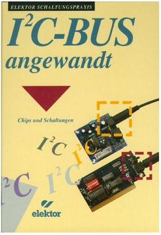
Think of it as a logic data book from the 70s, but for all possible I2C peripherals with sample circuits and sample
boards. If you are into retro-embedded systems, I highly recommend picking up a copy of this book (unfortunately, it’s in German).
With the book in hand, I made many trips to the local electronics store to pick up I2C chips and sensors. Back in the day,
you filled out an order form, talked to real folks at the store, and picked up your components a week or two later. It
wasn’t until the late 90s that the likes of Reichelt with large enough mail-in order paper catalogs
popped up in Germany to replace your local trusty electronics store.
Philips I2C Bus
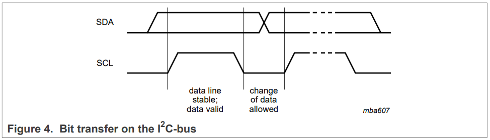
The bus uses two bidirectional open-drain lines, SDA and SCL, pulled up with resistors. Bit transfer is synchronized
by the clock line. Data is valid only when the clock line is high.
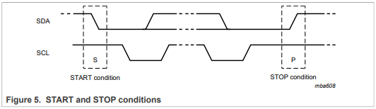
Transfers are framed by a start and stop condition. A high-to-low transition on the SDA line while SCL is high indicates
a start condition, while a low-to-high transition on the SDA line while SCL is high indicates a stop condition.
Between the start and stop conditions, data is transferred in 8-bit bytes, followed by an acknowledgment (ACK) bit.
The acknowledgment bit is generated by the receiver to indicate successful receipt of a byte. This is done by pulling
the SDA line low during the acknowledgment clock pulse. If the receiver does not pull the line low, it indicates a NACK (not acknowledged).
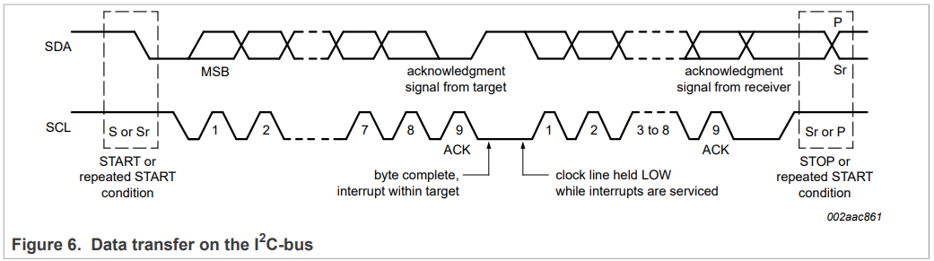
Since we can have many devices on the same bus, each device has a unique 7-bit address. The master initiates communication
by sending the 7-bit address of the target device, followed by a read/write bit. The addressed device responds with an
ACK if it is present on the bus. This allows us to connect multiple devices to the same two wires, and also enumerate
them without prior knowledge. This made I2C very popular for sensor networks and other applications where multiple peripherals
need to be connected to a single microcontroller, or multiple ICs need to be monitored on a computer motherboard (SMBus).
The I2C Specification has a good example of how a typical system
might look.
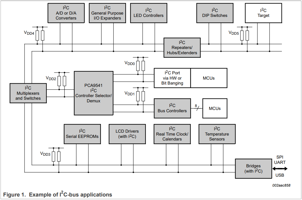
The number of devices on each branch is limited by the bus capacitance, which is typically around 400 pF. This usually
translates to about 10-20 devices per bus segment, depending on the specific devices used. To extend the bus, you can use
I2C bus extenders or repeaters.
Another consideration is the pull-up resistors. The value of the pull-up resistors affects the rise time of the
signals on the bus, which is affected by the bus capacitance. Texas Instruments has a good application note on selecting pull-up resistors for I2C buses. As a rule of thumb, for standard mode (100 kbps),
a pull-up resistor value of 4.7 kOhm is commonly used. For higher speeds, lower values may be necessary to achieve the required rise times.
While the specification on bus capacitance is fairly tight, in practice, you can often play fast and loose with the pull-up
resistors, at the risk of being bitten by occasional timing issues and becoming slave device dependent.
Given that we are bit-banging I2C on an archaic MCS-51 core, we will stick to standard mode speeds to keep timing manageable.
Atmel (aka Microchip) AT24C02 EEPROM
One of the most common I2C peripherals is the EEPROM (Electrically Erasable Programmable Read-Only Memory). Atmel (now Microchip)
produced a popular series of I2C EEPROMs, including the AT24C02, which provides 2 kilobits (256 bytes) of non-volatile storage.
While these were very common in the 90s and early 2000s for storing configuration data, calibration data, and other small amounts of data,
they have largely been supplanted by flash memory and other non-volatile storage technologies in modern systems. Especially
with the rise of microcontrollers with built-in in-system programmable flash memory and dramatic improvements in flash
endurance over the years, the need for separate EEPROM chips has diminished.
While flash has been around since the 80s, it was relatively expensive and had limited write endurance compared to EEPROMs.
Another issue was that you needed a high-voltage programming supply (12V or higher) to program early flash memory chips,
which made them less convenient and almost impossible to use in-circuit. Even the AT89C52 series microcontrollers with
on-chip flash required a special programming mode with higher voltages. However, as flash technology improved and costs decreased,
flash memory became more prevalent in embedded systems. My former embedded mentor and boss had his own website in the 90s and early 2000s explaining how folks could build flash programmers for the 89C2051 series microcontrollers on a dime. While not explicitly linked from the landing page anymore, you can still find
it hosted from his previous job.
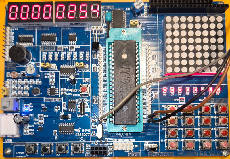
Anyway, I digress; the HC6800-ES2 development board includes an AT24C02 EEPROM connected to the I2C bus. The chip is
connected with the following pin configuration.
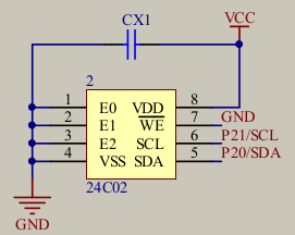
There are no explicit pull-ups for I2C on the board; instead, we solely rely on the bank of 10 kOhm resistors connected
to all GPIO pins. So the makers certainly did not expect high-speed I2C operation. P2.1 and P2.0 are used for SCL and SDA, respectively. None of these pins have any alternate functions that are going to be useful for us, so we have
to bit-bang the protocol entirely in software.
The connection and start and stop conditions are straightforward to implement. We just need to set and clear the appropriate
pins with appropriate delays to meet the timing requirements.
#define I2C_SCL P2_1
#define I2C_SDA P2_0

#define DELAY_10US() NOP(); NOP(); NOP(); NOP(); NOP(); NOP(); NOP(); NOP(); NOP(); NOP()

void i2c_start(void) {
  I2C_SDA = 1;
  I2C_SCL = 1;
  DELAY_10US();
  I2C_SDA = 0;
  DELAY_10US();
  I2C_SCL = 0;
  DELAY_10US();
}

void i2c_stop(void) {
  I2C_SDA = 0;
  DELAY_10US();
  I2C_SCL = 1;
  DELAY_10US();
  I2C_SDA = 1;
  DELAY_10US();
}
Transferring bytes is a bit more involved. We need to shift out each bit of the byte, starting with the most significant bit (MSB).
Then we need to check for the acknowledgment bit from the slave device.
uint8_t i2c_write(uint8_t byte) {
uint8_t timer = 0;
for(uint8_t i = 0; i < 8; i++) {
I2C_SDA = byte >> 7;
byte <<= 1;
DELAY_10US();
I2C_SCL = 1;
DELAY_10US();
I2C_SCL = 0;
DELAY_10US();
}
I2C_SDA = 1;
DELAY_10US();
I2C_SCL = 1;
while(I2C_SDA) {
timer++;
if(timer > 250) {
I2C_SCL = 0;
DELAY_10US();
return 0;
}
}
I2C_SCL = 0;
DELAY_10US();
return 1;
}
Reading a byte is similar, but we do not have to worry about the ACK bit for now.
uint8_t i2c_read() {
  uint8_t byte = 0;
  for(uint8_t i = 0; i < 8; i++) {
    I2C_SCL = 1;
    DELAY_10US();
    byte |= I2C_SDA;
    I2C_SCL = 0;
    DELAY_10US();
    byte <<= 1;
  }
  return byte;
}
With these building blocks, we can now implement higher-level functions to read and write data to the AT24C02 EEPROM.
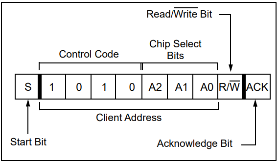
Addressing the AT24C02 is straightforward. The device has a 7-bit I2C address of 0x50 (1010000 in binary), plus
whatever the address lines are set to. On the HC6800-ES2 board, all address lines are tied to ground (E0..E2), so the
full 8-bit address for writing is 0xA0 (0b10100000 in binary) and for reading is 0xA1 (0b10100001 in binary).
The AT24C02 is byte addressable, meaning that you can read and write individual bytes at specific addresses. That makes
the interface straightforward. Here is a simple implementation of reading and writing a byte to the EEPROM.
#define AT24C02_ADDR 0xA0
void at24c02_write_byte(uint8_t mem_addr, uint8_t data) {
i2c_start();
i2c_write(AT24C02_ADDR);
i2c_write(mem_addr);
i2c_write(data);
i2c_stop();
}
uint8_t at24c02_read_byte(uint8_t mem_addr) {
uint8_t data = 0;
i2c_start();
i2c_write(AT24C02_ADDR);
i2c_write(mem_addr);
i2c_start();
i2c_write(AT24C02_ADDR | 0x01);
data = i2c_read();
i2c_stop();
return data;
}
Now we just need to make it interactive. Looking at the dev-kit, we can use the buttons K3 and K4. If we press K3, we write a value to the EEPROM at address 0x00. If we press K4, we read the value back and display it on the
7-segment display.
#define K3 P3_2
#define K4 P3_3

void main(void) {
  timer0_init();
  EA = 1; // Enable global interrupts
  ET0 = 1;	/* Enable Timer 0 interrupt */

  for(;;) {
    if(!K3) { // Write current_value to address 0x00 on button press
      delay(5000); // Debounce delay
      if(!K3) { // Confirm button still pressed
        EA = 0; // Disable global interrupts
        at24c02_write_byte(0x00, 0xFF);
        EA = 1; // Enable global interrupts
        while (!K3); // Wait for button release
      }
    }
    if(!K4) { // Read byte from address 0x00 on button press
      delay(5000); // Debounce delay
      if(!K4) { // Confirm button still pressed
        EA = 0; // Disable global interrupts
        uint8_t data = at24c02_read_byte(0x00);
        EA = 1; // Enable global interrupts
        int_to_digits(data, digits);
        while (!K4); // Wait for button release
      }
    }
  }
}
The layout and the really large pull-up resistors on the dev-kit make for a pretty slow and noisy I2C bus. This is not
the best I2C implementation ever, but it works reliably enough for demonstration purposes.
The full source code with the 7-segment display multiplexing can be found on GitHub. As with the previous
implementation of the Dallas 1-Wire protocol, the logic analyzer comes in handy to debug and verify
the I2C bus transactions.
Published: 2025-11-23
Updated : 2025-11-23
Not a spam bot? Want to leave comments or provide editorial guidance? Please click any
of the social links below and make an effort to connect. I promise I read all messages and
will respond at my choosing.