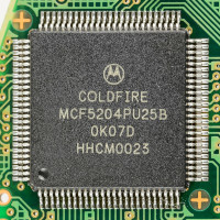
I am currently TAing SE350. The students’ deliverable is a small real-time executive kernel (RTX) that runs on a Freescale Coldfire chip. We got the idea of building an automated embedded test suite for the students’ term projects.
However, instead of having to compile the students’ code from scratch, we would only want to take their firmware binary
directly and test it. This testing would involve injecting several test processes into the students’ OS. These tests would
stress their implementation and dump the results to a serial port of the actual Coldfire board. Having worked in the
embedded field, this problem is similar to integrating bootloaders with firmware. In the project, the bootloader is
the testing code and the actual firmware is the code to be tested.
You end up with two pieces of binary code that will be programmed into your device. So the challenge is to make them
talk to each other. In the case of the bootloader, you have the bootloader invoking the firmware, and in the case of
the testing code, the testing code invokes the RTX.
In the following sections, I describe the steps for:
- Building a toolchain,
- Developing the bootloader and firmware code,
- And integrating the different SREC/S19 files
In the second part, I will describe how to leverage the established framework to design a native testing suite.
In order to run code on bare (i.e., no existing OS) chips, you need to have a toolchain that translates your source
code into ELF files (ELF = Executable and Linkable Format) and SREC/S19 files for flashing onto the device. We need:
A detailed description of how to build these tools is already here on my website.
Step 2: Where to Put My Firmware Code?
If you are going to integrate two pieces of code, you need to make sure they do not overlap in flash and do not access
each other in an undesired fashion. Since you are developing on the bare hardware, you actually have complete control
over the former property and can enforce the latter by careful code design. Your generated ELF file will consist of
three major sections, as follows:
- The text segment
(.text), where your executable code goes, - The data segment
(.data), where initialized global variables go, - The BSS segment
(.bss), where uninitialized global variables go.
Note that the BSS segment exists for some historic reason, and in almost all OS lectures it is implied by the data segment (i.e., data := data + BSS). By convention, the text segment starts at a lower address than the data and BSS segments.
When your program is executed, the values of the data and BSS segments are copied into the main memory. However,
the size is not established at runtime. The program’s stack for function calls and local variables resides on the heap,
which is by convention allocated after the BSS segment and grows dynamically. The GNU toolchain you just built includes
the GNU Linker, which allows specifying these locations explicitly by linker scripts (i.e., LD files). GNU LD files have
a simple structure describing:
- The memory banks and locations,
- How to spread your code across those locations.
The following simple example file describes an embedded system (i.e., in my case: CJDesign’s MCF5307 board). Most
evaluation boards, like mine, come with a huge SRAM and actually have a ROM that allows you to load code into main
memory. As such, we will dump all code into SRAM for testing purposes. The following example specifies the assignment
of 1 MB at address 0x10100000 to SRAM and dumps all sections of the code into that segment. Hint: the space after the
section names is required to ensure the uniqueness of the names. The actual code will execute from the SRAM start
address, which is 0x10100000.
MEMORY
{
sram : ORIGIN = 0x10100000, LENGTH = 1M
}
SECTIONS
{
.text :
{
*(.text)
*(.rodata*)
} > sram
.data :
{
*(.data)
} > sram
.bss :
{
*(.bss)
} > sram
}
A note for SE350 students: Please do not attempt to hack the linker file provided by the course. You may run into
serious trouble by using my linker script or hacking the existing one!
Step 3: Building Your Firmware
To compile and link your source (firmware.c) with this file, use the following command:
m68k-elf-gcc -Tfirmware.ld -Map=firmware.map -o firmware.elf firmware.c
You may want to generate a listing of the file to see that everything is at the expected location, as follows:
m68k-elf-objdump -xdC firmware.elf > firmware.lst
In order to flash or deliver this file to the customer, we actually need to convert it into the Motorola S19/SREC file
as follows:
m68k-elf-objcopy --output-format=srec firmware.elf firmware.s19
Step 4: Building the Other Piece of Code
What’s left to build is the bootloader. In order to ensure distinct flash and memory regions, you need to provide another
linker script that puts all the bootloader code into a different location than the other code. A wise choice is to put
this code as far away from the actual firmware as possible, possibly at the end of the available memory. The following
code offsets the memory bank by 1MB and dumps the code there.
MEMORY
{
sram : ORIGIN = 0x10200000, LENGTH = 1M
}
__FIRMWARE__ = 0x10100000;
SECTIONS
{
.text :
{
*(.text)
*(.rodata*)
} > sram
.data :
{
*(.data)
} > sram
.bss :
{
*(.bss)
} > sram
}
In order to invoke the firmware, we need to put a symbol inside the linker script that identifies the expected starting
address of the firmware, which is in this case called firmware. This symbol can be used from the C code directly as a
function call. In order to avoid any compilation warnings, you should forward declare this function as external. The
compilation and transformation into the S19 file is analogous to creating the firmware code. You should end up with a bootloader.s19.
Step 5: Throwing Things Together
In practice, when you build an embedded device, it should have the bootloader and some firmware programmed in when it
leaves assembly. In many cases, the interface that the end-user has to the device (i.e., a USB connector) is different
from what you have during assembly (e.g., an in-system flash tool). As such, it is necessary to combine the bootloader
and the firmware together.
The S19 format is a simple ASCII data exchange format, originally developed by Motorola, for executable code.
It is widely accepted by most programmers for Motorola-based embedded systems. The files are processed line by line;
each line contains a control code, a record size, an address, an optional data sequence, and a checksum. You can find the
details here.
GNU Object Copy usually outputs:
- A block header (
S0), - A sequence of data records (
S1-S3), - And the start address (
S5-S9).
The block header usually contains the name of the file (e.g., firmware.s19 or bootloader.s19). Most ROM loaders on
evaluation boards will actually process the start address record, which is in our case the declared origin of the SRAM,
and fail to load if they do not find it, so it needs to be included.
So in order to put the bootloader and the firmware together into one file, you need to provide one header, the data of
both programs, and one starting address:
- Header: any of the firmware/bootloader, or a custom header (see below)
- Data: concatenate the data records of both original programs
- Starting address: the start address of the bootloader
Yes, geeky people like me actually enjoy implementing checksum algorithms and branding their creation. In order to do so, we
need to dive into the checksum procedure used by S-records. According to Wikipedia, the checksum is
”[…] the least significant byte of ones’ complement of the sum of the values represented by the two hex digit pairs
for the byte count, address and data fields.” So guys, it’s time to dig out those algorithm-class notes and figure that
out, … oh wait …, found it:
- Sum up all bytes starting from the byte count record.
- Set:
checksum = 0xFF – (0x00FF & sum)
Why the hell would anyone use such a checksumming algorithm? The answer is simple: It can be easily checked!
While processing the S19 records, you can actually sum everything up, including the provided checksum, and should get
0xFF. That is a simple compare operation and can be evaluated in no time.
Step 6: Testing Your Creation
If you build the Coldfire simulator according to my instructions, you can invoke the simulator as follows:
coldfire --board cjdesign-5307.board
and load the code like this:
Use CTRL-C (SIGINT) to cause autovector interrupt 7 (return to monitor)
Loading memory modules...
Loading board configuration...
Opened [/usr/local/coldfire/share/coldfire/cjdesign-5307.board]
Board ID: CJDesign
CPU: 5307 (Motorola Coldfire 5307)
unimplemented instructions: CPUSHL PULSE WDDATA WDEBUG
69 instructions registered
building instruction cache... done.

Memory segments: dram  timer0  timer1  uart0(on port 5206)
uart1(on port 5207)  sim  flash  sram
Remember to telnet to the above ports if you want to see any output!
Hard Reset...
Initializing monitor...
Enter 'help' for help.
dBug> dl merged.s19
Downloading S-Record...
Done downloading S-Record.

dBug> go 0x10100000 <- the actual firmware
... some garbage, because RTS returns to nowhere...
dBug> go 0x10200000 <- the boot-loader invoking the firmware
You should yield the following output on the terminal (telnet localhost 5206).
Trying ::1...
Trying 127.0.0.1...
Connected to localhost.
Escape character is '^]'.

uart0
Inside firmware! <- 1st go of the firmware
Inside bootloader! <- 2nd go inside firmware!
Inside firmware!
Back in bootloader!
Discussion
In this part of the how-to, I explained the basics of building two pieces of binary Coldfire code and integrating them
into a single file that can be processed by most programmers and ROM loaders. A popular application is the integration
of bootloader and firmware code for embedded system assembly. Another application is embedded grey-box testing. In this
technique, instead of a bootloader, a test suite is evaluated against the firmware to check for potential defects. In
the next post, I’ll describe how to design such a test framework.
You can find the sample code for this post below. The code will contain some modified linker scripts that deal with
particular alignment problems of the simulator. Furthermore, the bootloader and the firmware should have different
stacks, so some assembly files have been added to do so. The S19 merging is done by the Python script merge.py.
Cross posted from my old Blog
Published: 2010-02-06
Updated : 2025-10-04
Not a spam bot? Want to leave comments or provide editorial guidance? Please click any
of the social links below and make an effort to connect. I promise I read all messages and
will respond at my choosing.